
LeCroy AP031 Differential Probe
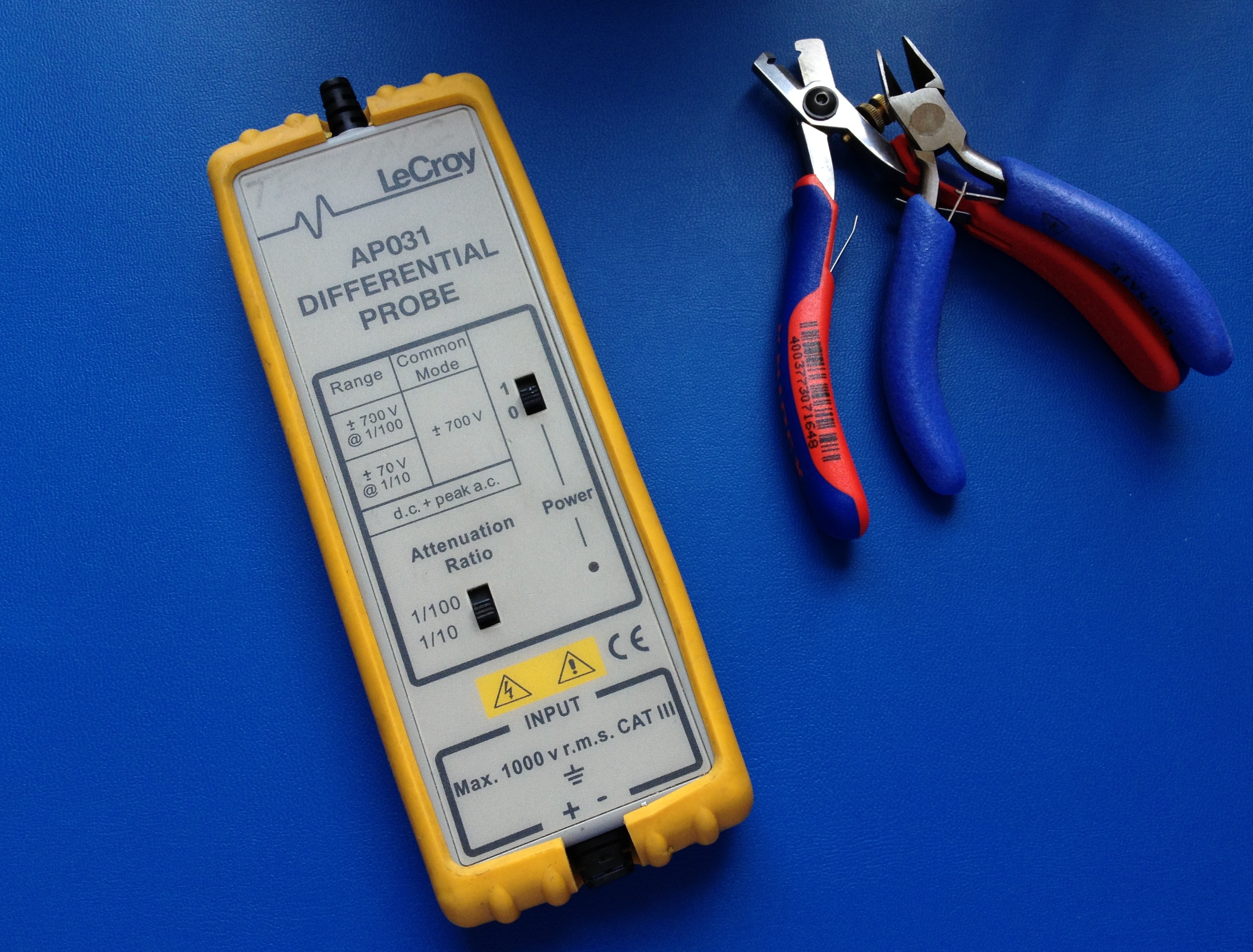
LeCroy AP031 Differential Probe. Nearly as received, cables cut.
While setting up my lab, I’ve been reading about safety when making measurements using oscilloscopes. At first I was planning on wiring up my bench with a few isolated outlets (via an isolation transformer). Or using a GFCI to try and protect me from toasting myself when poking around off line regulators. I kept reading, and decided that the pitfalls associated with isolation transformers were easily overcome through the use of an active high-voltage differential probe.
I was, at first, planning on putting together my own active HV probe, and was curious what the pros do when isolating and dividing down the test signal. I was browsing around that big internet yard sale and I found a LeCroy AP031 differential high-voltage probe for $25, totally broken. I figured I’d have a look at how it was designed to build my own. While tearing it down, I decided to detour a bit and try to fix it.
The AP031 is an odd beast. It’s clearly not designed or built by LeCroy. A casual search finds a number of other manufacturers offering it as their own such as the Picotech TA041, Siglent DPB425, Probe Master 4231, Pintech PT8001, Kaltman Creations ADP1, and the TPI ADF25A.
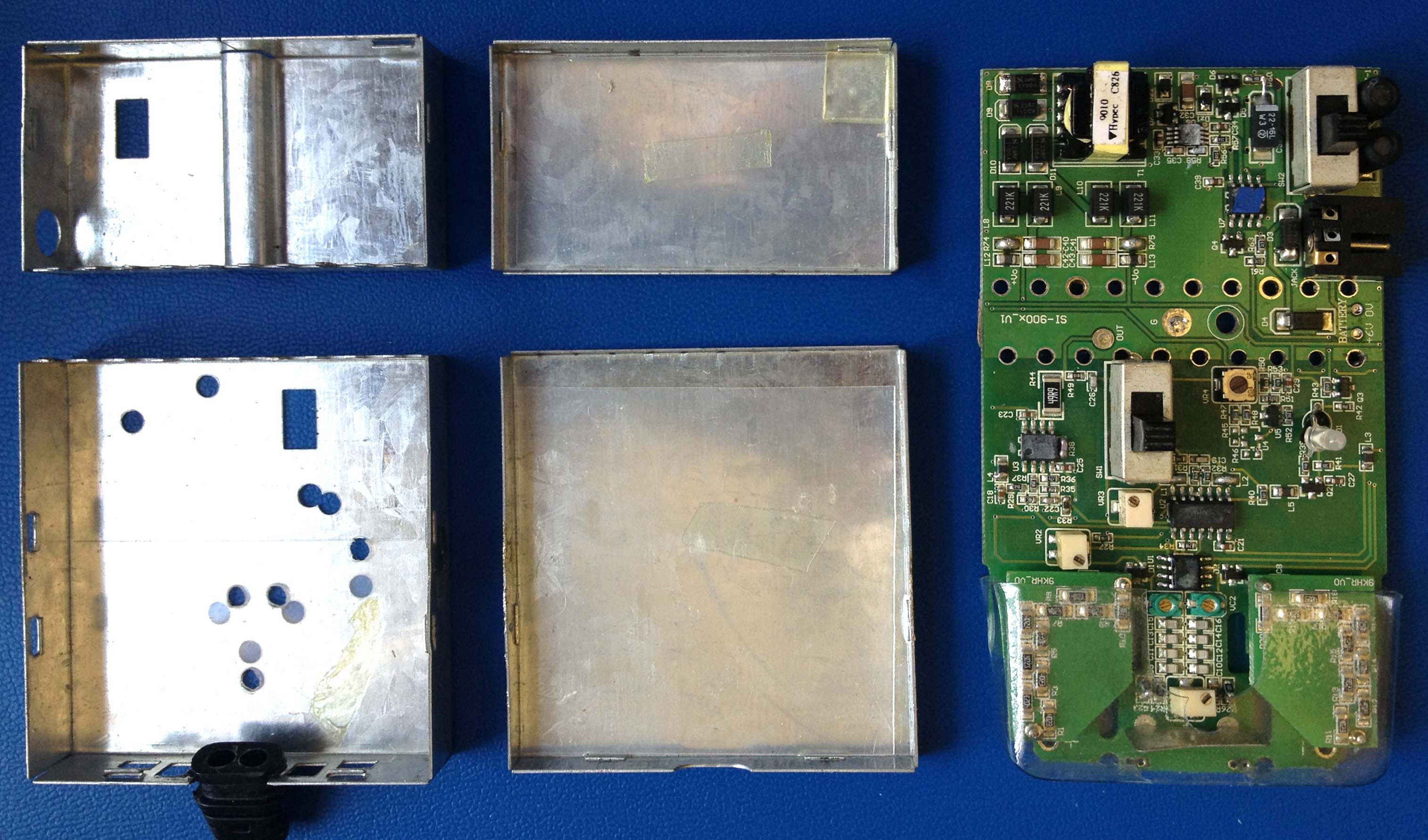
LeCroy AP031 differential probe exposed.
Once the yellow rubber boot was removed, the battery cover and batteries were removed revealing two screws. With those screws removed, using a hard nylon spudger, the case was unsnapped. Inside the case, two shielded areas are apparent. The shielded region closest to the signal input is the analog section. The shielded region closest to the batteries is the power supply section.
The designers clearly paid somewhat nice attention to detail. All the shields are insulated internally to guard against shorts. Small plastic blocks have been glued all around the boards to keep the shields from coming into contact with the circuit boards. There is a nice cutout for the signal coax and the power wires to pass to the rear of the unit. There is an additional plastic shield around the signal input to guard against shorts.
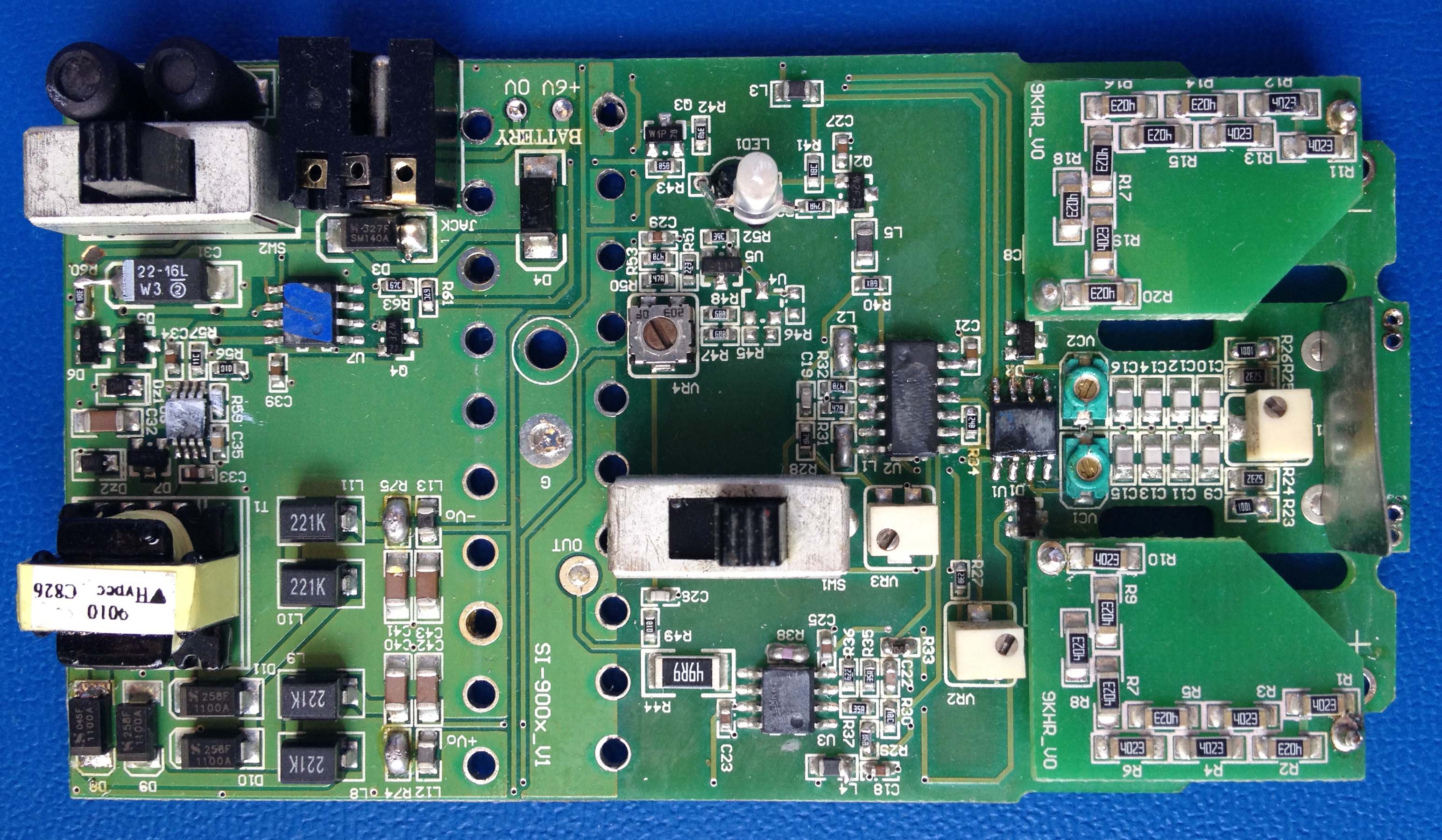
LeCroy AP031 circuit board. All the numbers on the chips are rubbed off!
ARGH! Every single chip in the probe has had it’s part number scrubbed off, and many of them have had some paint applied over that! Whyyy! Well probably because it would be pretty easy to build a clone if they hadn’t. Still, that sucks for repairs.
In the image above, the signal enters the unit on the left. The boards stacked above with a string of resistors for the divider network for the probe. Underneath the resistor boards is a similar string of series capacitors to compensate the network for high frequency operation. From there, the signal passes into U1, what one can only assume to be an amplifier – though the pinout is not similar to a common op-amp. There’s a capacitor / resistor network surrounding it to trim gain and presumably CMRR.
The trim pot VR1 in this network was broken off. Presumably, the input leads were pushed into the unit, which hit the (flimsy) shield, tearing off the front of the potentiometer. Hopefully that’s what caused this unit to be junked, not something to do with the mystery ICs.
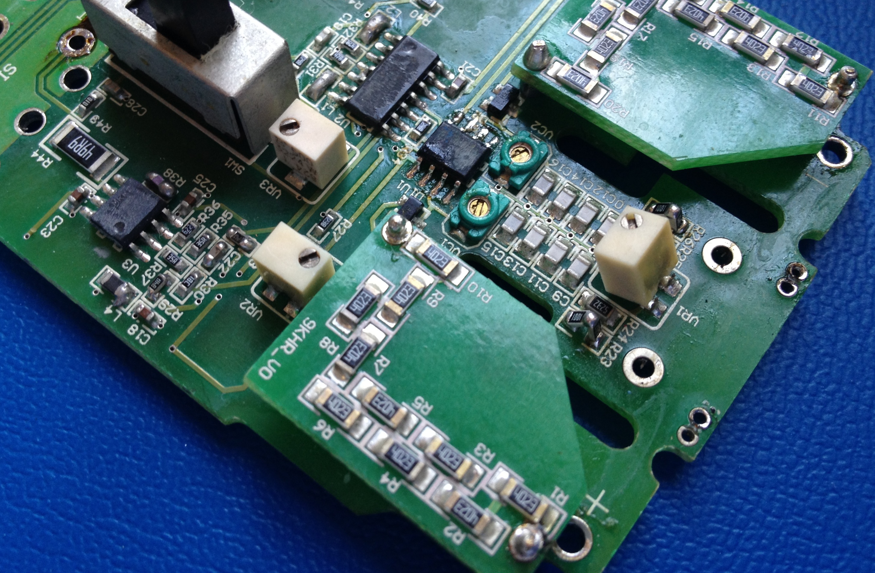
Broken off pot. Note creative soldering on R23 and R26.
From, U1, the signal is further amplified by U2, what looks to be a quad op-amp. The other amplifiers in U2 appear to be used to generate a split power supply for U1 and U3. Note L1 and L2 are bridged by a solder blob. They were most likely intended to provide additional supply filtering. U3 appears to be simply a line driver. Note the massive 49.9 ohm resistor R44 for output impedance matching.
In the power supply section, we first see a reverse protection diode D4. U7 with Q4 could be an ideal diode controller to select between batteries and the wall adapter source. U6 looks to be a switch-mode supply controller. Following the transformer are rectifiers and LC filters for the positive and negative rails. There’s a pretty serious amount of filtering and regulation on the power supplies – which makes sense considering the application. It’s fairly audacious to use a switching power supply in an oscilloscope probe.
Finally, U5 appears to be a supervisory voltage monitor similar to a TPS3809. This drives the LED, indicating if the probe is running low on batteries.
What’s Next?
I replaced the pot, added leads, and output coax. I was gonna measure the resistance of the pot that I removed, but the leads were broken off. Scraping off some resin and trying to probe the substrate said the pot was set to full scale, probably not correct, so that’ll require some tweaking once it’s together. Somewhere I found the calibration process for this probe, which I cannot find again. I thought it was on the Probemaster website, but it has either been removed from there, or it’s been removed from my memory.
As part of this, next I’ll probably build a (moderately) high voltage square wave generator for use in calibration. I was thinking I could use a high voltage op-amp like a LTC6090 or a OPA454. I’ll post again when it comes time to calibrate it.
Qno on the eevblog forum[1] pointed me towards who appears to be the actual OEM for the probe, Sapphire.tw who’s got both a user manual [2] and a calibration manual [3]. Fantastic!
[1] http://www.eevblog.com/forum/testgear/lecroy-25mhz-hv-differential-probe-teardown-repair/msg278233
[2] http://www.sapphire.com.tw/manual/9001um.pdf
[3] http://www.sapphire.com.tw/manual/9001cp.pdf
Underwurlde on the eevblog forum claims to have reverse engineered[1] the probes. He reports the input device, U1, is a SST441 dual JFET which is buffered by U2, a LM3046 transistor array. He reports the output buffer U3 is a vanilla 741. At first glance, his claims appear correct, though I have not dug too deeply.
[1] http://www.eevblog.com/forum/testgear/probe-master-differential-probes-anyone-used-these/msg351503/#msg351503
Hello!
Yes, that was me that rev-eng’d those probes (two types: surface mount type and through-hole components type): Link to better, more up to date schematics.
http://www.diyaudio.com/forums/equipment-tools/248505-differential-probe-reverese-engineered.html
The supply ‘supervisor’ is nothing more than what would appear to be a dual comparitor btw (not sure, but pin-out & surrounding connected devices suggest this).
Andy
The calibration procedure can be found here:
http://www.sapphire.com.tw/manual/9001cp.pdf
or
http://www.sapphire.com.tw/si9001cp.htm
Hi there,
i could actually read the part number o U3 in my broken AP031 – its a nat semi LM6365M
And U4 is (i assume CMOS) simply a 555 timer press-ganged into service as an SMPS controller.
thanks for the useful data!
Andy,
Nice work…
I am setting up a home lab to be able to design and test switched mode power supplies (low power… <50W) and run different experiments on them to… learn more in depth.
I understand your project was started to calibrate and repair the probes; however,
did you ever attempt to build one from scratch?
do you know how many layers are in the PCB?
are you aware of any gerber files for this around?