Instek GDS-820C Teardown
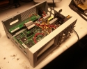
Teardown of the Instek GDS-820C oscilloscope on a lazy Friday afternoon.
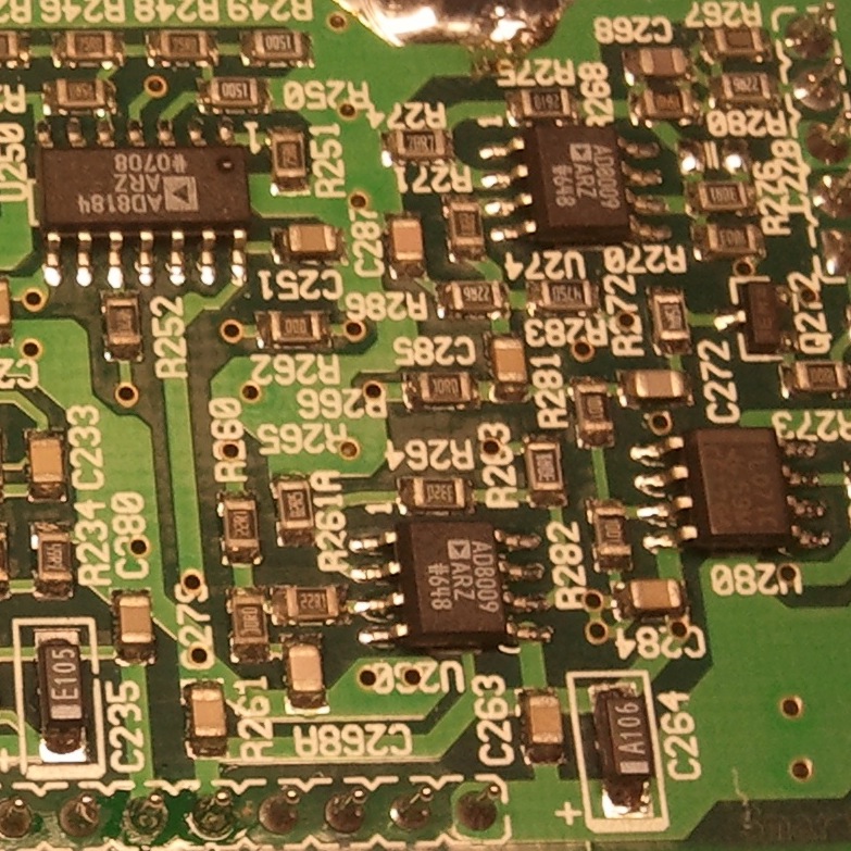
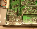
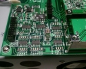
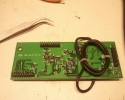
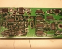
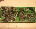
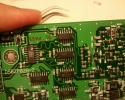
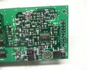
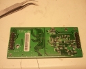
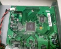
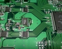
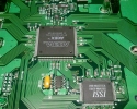
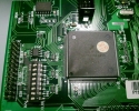
It’s a fairly interesting design, two layer boards, no parts are leadless. The finest pitch components are the Altera FPGA and the Freescale CPU. Definitely “older” technology than a modern Tek or Agilent scope. Looks like a prototype I might build. It’s a good design to look at for inspiration.
Some highlights
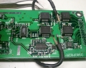
- The scope claims a 150MHz analog bandwith with “ET25GS/s”, it has a pair of 100MS/s Analog Devices AD9283 analog to digital converters
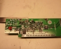
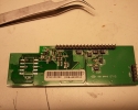
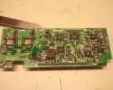
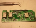
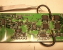
- There is a trigger daughter card that has a delay line made of coiled coax
- Many of the high speed analog cards – the input boards, trigger stuff – are labeled “SparkGap” rather than Instek
- There is a configuration dip switch on the board which controls the display and UI with silkscreen marks indicating which options the scope has
In the future, I may reverse engineer the input signal chain.


I was looking around for examples of products with FPGAs in them and wouldn’t you know it, it’s my old friend Andy.
Hi, do you know what kind of LCD is there, and what interface is used with the CPU?
Thank you very much!